Intel 80486
Intel’s 80486, introduced in 1989, integrated a 32-bit CPU, 8 KB cache, and floating-point unit onto a single die, marking the first x86 processor to combine all three, drastically reducing interchip latency compared to the 386/387 pairing
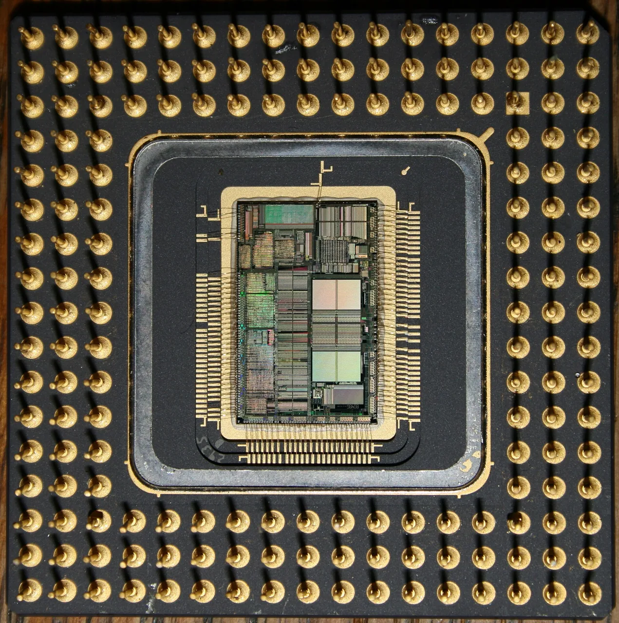
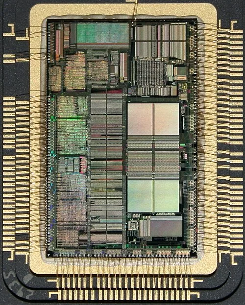
The 80486 represented a structural shift in x86 design, advancing beyond a simple increase in clock speed. By incorporating an 8 KB, 2-way set associative cache that used a write-through policy, along with a full floating-point unit on-die, the 80486 eliminated the performance bottleneck of external math coprocessors13. This integration cut interchip delays inherent in the 386 and 387 multichip configuration, delivering reportedly two to four times the throughput of a standard 386 system12. The chip housed approximately 1.2 million transistors, a threshold noted in pre-release coverage as a symbolic milestone in VLSI complexity312.
Architecturally, the 80486 implemented a superset of the 80386 instruction set and maintained total backward compatibility with earlier x86 processors, ensuring reliable operation under DOS, OS/2, and Novell NetWare181011. It was also promoted as optimized for XENIX and UNIX environments8. The processor featured a full 32-bit internal and external data bus, a 32-bit address bus supporting up to 4 GB of physical memory, and native handling of 8-, 16-, and 32-bit data types3.
Product Line Variants
The 80486DX was the flagship model, available at clock rates of 25, 33, and 50 MHz, and included both the integrated math coprocessor and 8 KB cache12. In contrast, the 80486SX omitted the floating-point unit and was paired with a separate 80487SX coprocessor3. The SX was offered at 20, 25, and 33 MHz2. The 80486DX2 used a clock-doubling design, with internal speeds of 50 or 66 MHz while running on 25 or 33 MHz external buses2. The 80486DX4, 80486SL, 486SX2, and 80487 coprocessor are indexed in documentation but lack detailed specifications in the source material45.
Design & Debugging
Intel produced bondout versions of the 80486, known as In-Circuit Emulator (ICE) variants, which featured additional pins for real-time debugging and trace analysis1. These were intended for use with emulator hardware during system development. The architectural refinement over the 386 extended beyond integration; microcode and hardware execution paths were optimized to enhance instruction throughput, though the exact nature of these improvements is not detailed in the sources1.
Market Rollout
Pre-release reports from 1989 indicated Intel was finalizing the 80486 design and intended to launch it that year12. Desktop adoption was anticipated to begin one to two years post-introduction, reflecting the typical lag between CPU availability and system integration12. No original pricing data survives in the source set, and the exact release date within 1989 is unspecified.
Specifications
| Clock rate | 25 – 50 MHz (DX); 20 – 33 MHz (SX); 50/25 – 66/33 MHz (DX2) |
| Transistor count | 1.2 million |
| Internal data bus | 32-bit |
| External data bus | 32-bit |
| Address bus | 32-bit |
| Physical memory support | 4 GB |
| Data types | 8, 16, 32 bits |
| Cache | 8 KB, 2-way set associative, write-through policy |
| Floating-point unit | Integrated in DX; absent in SX |
| Instruction set | Superset of 80386 |
| Compatibility | DOS, OS/2, NetWare, XENIX/UNIX |
References
- TheUndocumentedPCSecondEdition FrankvanGilluwe
- GG24-4002-0 IBM PS 2 and PS ValuePoint Subsystems Dec92
- The 80x86 IBM PC and Compatible Computers - 4th Edition
- URP 8th edition
- URP 6th edition
- 1989 12 BYTE 14-12 5 New Laptops and Sound Image Processing and Case Tools (1989)
- GG24-3775-00 OS2 V2.0 Vol 5 Print Subsystem 199208 (1992)
- GG24-3730-00 OS2 V2.0 Vol 1 Control Program 199204 (1992)
- URP 1st edition