Intel 8085
Intel’s 8085 was an 8-bit NMOS CPU that consolidated key system components of the 8080A into a single chip, enabling compact designs while maintaining full software compatibility with its predecessor.
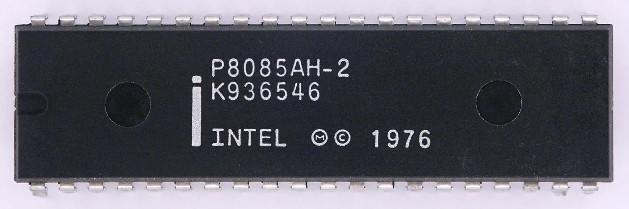
The 8085 emerged as a system-level refinement of the 8080A architecture, integrating functions previously handled by discrete support chips. Unlike the 8080A, which required the 8224 clock generator and 8228 system controller to form a functional core, the 8085AH incorporated these elements internally, reducing component count and simplifying board layout3. This consolidation allowed for a minimum viable system using just three ICs: the 8085AH itself, the 8156H (providing RAM and I/O), and the 8355 or 8755A (delivering ROM/PROM and additional I/O)3. The design prioritized integration without sacrificing expandability, a principle emphasized in Intel’s own documentation, which stated “maintaining total system expandability” despite the reduced chip count3.
Operationally, the 8085 ran on a +5V supply and employed N-channel depletion-load silicon gate technology (HMolS), a process choice that contributed to its speed and power efficiency for the era3. It featured an internal clock generator, eliminating the need for external clock circuitry in many applications2. While the base model’s exact maximum clock speed is not explicitly documented in surviving sources, a Space Byte implementation operated at 3MHz using 450ns memory, implying tight timing margins6. The minimum instruction cycle time was 1.302 microseconds, aligning with a minimum clock period of 1.3µs as noted in the Towers International Microprocessor Selector62. Later variants, the 8085AH-1 and 8085AH-2, were explicitly marketed as faster iterations of the original 8085AH, though specific performance figures remain undocumented3.
Software continuity was a cornerstone of the 8085’s value proposition. Its instruction set was 100% software compatible with the 8080A, allowing direct reuse of existing codebases3. Development tools reflected this duality: assemblers such as ISIS-II 8080/8085 ASSEM. V2.0 accepted source code for both processors9, and programming manuals like the Intel 8080/8085 Assembly Language Programming Manual treated them as a unified target15. Even higher-level tools, including the PL/M-86 compiler suite and 8086 Family Utilities, supported 8080/8085-based development systems14. The SDK85 Monitor, provided with Intel’s System Design Kit, offered a hands-on environment for debugging and prototyping9. CP/M ran effectively on the 8085 due to binary compatibility, cementing the chip’s role in early microcomputing ecosystems16.
Second sourcing ensured broader availability, with Advanced Micro Devices listed as a licensed manufacturer2. The processor was offered in both standard and extended temperature ranges, suggesting industrial and embedded applications beyond hobbyist use3. Packaging options included “EXPRESS,” though the nature of this variant (whether delivery format, packaging type, or configuration) is not clarified in available sources3. Boards like the CompuPro CPU 8085/88 combined the 8085 with the 8088, offering switch-selectable clock speeds of 2 or 6 MHz, indicating system-level flexibility even if the base CPU’s native limits are ambiguous4.
The 8085 was not a radical departure, but a pragmatic evolution, engineered for designers who needed the 8080’s software base in a simpler, more integrated package. Its lack of a documented release year, pricing, or transistor count in surviving materials suggests that Intel positioned it less as a standalone milestone and more as a functional upgrade within the MCS-80/85 family15. Manuals such as the MCS-85 Users Manual and the Intel 8085 User Manual provided detailed operational guidance, reinforcing its role as a tool for engineers rather than a consumer-facing product71011. In an era when every gate counted, the 8085’s integration made it a quiet workhorse, unflashy but deeply practical.
Specifications
| Data width | 8 bit |
| Technology | N-channel, depletion load, silicon gate (HMolS) |
| Supply voltage | +5V |
| Minimum clock period | 1.3 µs |
| Memory addressing | 64K bytes |
| Instruction set compatibility | 100% software compatible with 8080A |
| System integration | Includes functions of 8224 clock generator and 8228 system controller |
| Minimum system configuration | 8085AH (CPU), 8156H (RAM/IO), 8355/8755A (ROM/PROM/IO) |
| Temperature ranges | Standard and Extended |
| Second sources | Advanced Micro Devices |
| Available in | EXPRESS |
References
- 9800301-04 8080 8085 Assembly Language Programming Manual May81
- Towers International Microprocessor Selector
- Microprocessor Data Hand Book
- CompuProProductData
- 210621-031 Intel Literature Guide Dec88
- The itty bitty machine company Winter 1977 Catalog (1977)
- 1980 08 BYTE 05-08 The Forth Language (1980)
- INSITE pgmLibrManVol2 Aug79
- INSITE pgmLibrManVol1 Aug79
- 1980 11 BYTE 05-11 High-Resolution Graphics (1980)
- 1980 09 BYTE 05-09 Homebrewing (1980)
- MICRO Vol46-03 82
- 121575-003 Intellec III Product Overview Sep82
- 9800478-04 PLM-86 Compiler Operating Instructions for 8080 Development Systems Aug80
- 9800616-03 iSBC 544 Intelligent Communications Controller Apr84
- 1983 03 BYTE 08-03 Mass Storage (1983)