Intel Pentium Pro
Intel's sixth-generation x86 microprocessor, introduced in 1995, integrated a full-speed L2 cache in a dual-cavity package and redefined 32-bit server performance through aggressive micro-op translation and out-of-order execution.
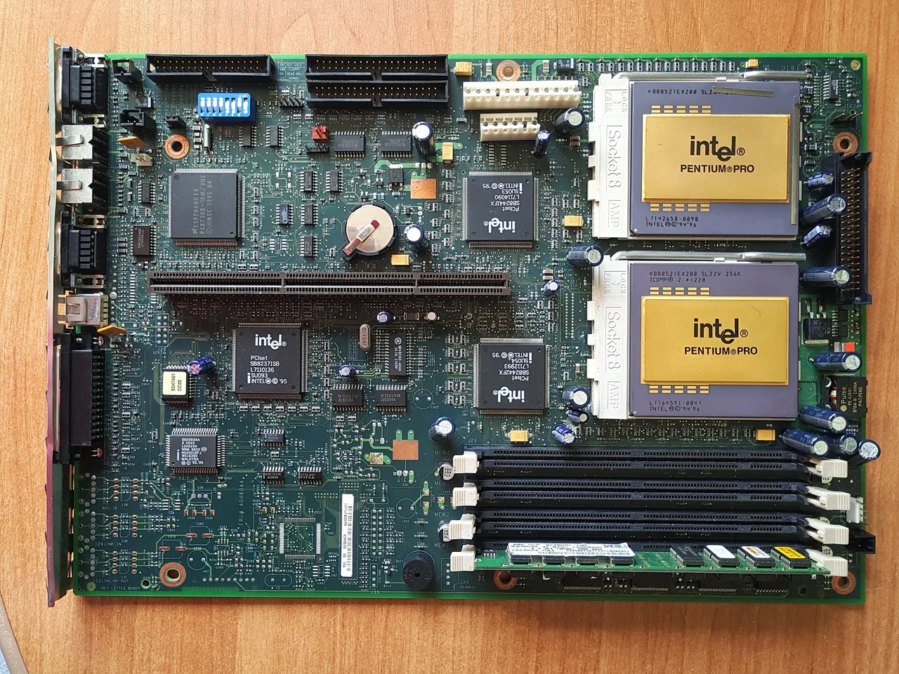
The Pentium Pro marked Intel’s formal embrace of RISC-inspired design, translating x86 instructions into micro-operations (uops) for internal execution, a departure from prior x86 implementations3. This translation layer, combined with three execution engines capable of retiring up to three uops per cycle, enabled significant throughput gains in 32-bit workloads8. The processor was explicitly optimized for 32-bit code, making it a natural fit for server and workstation environments running operating systems like Windows NT, with which it was frequently bundled8.
Physically, the Pentium Pro was housed in a 387-pin Dual Cavity PGA package measuring 2.46 × 2.66 inches (6.25 × 6.76 cm), with the processor die and L2 cache die stacked in separate cavities under a single lid2. This design allowed the L2 cache, available in 256KB, 512KB, or 1MB configurations, to run at full core speed over a dedicated 64-bit bus, eliminating the motherboard-level cache bottlenecks of Socket 7 designs12. The integration avoided cache coherency issues by keeping L1 and L2 caches private to each processor in multiprocessor systems12.
Despite its performance claims, Intel asserted the 133 MHz Pentium Pro was twice as fast as a 100 MHz Pentium. The chip faced architectural trade-offs6. Its deep pipeline and translation overhead resulted in subpar performance on 16-bit code, undermining its utility in mixed-mode environments such as Windows 95. The chip supported a 36-bit address bus, enabling access to 64GB of physical memory and 64TB of virtual memory, a substantial leap over prior generations258.
Intel launched the Pentium Pro for the server market, positioning it above the consumer-focused Pentium line8. It operated at initial clock speeds of 150 MHz and 166 MHz, later scaling to 180 MHz and 200 MHz, with clock multipliers of 2.5x and 3x258. At 150 MHz, it consumed 23 watts of power and ran on either 3.1v or 3.3v32. The processor was fabricated using multiple process technologies: 0.6-micron BiCMOS, 0.35-micron CMOS, and later 0.25-micron CMOS6.
Transistor count remains ambiguous in the documentation: one source cites 5.5 million, while another states 21 million, likely reflecting the inclusion or exclusion of L2 cache transistors38. The L2 cache alone added 15.5 million (256KB), 31 million (512KB), or 62 million (1MB) transistors, supporting the higher figure when cache is included5.
Intel supplied the 450KX/GX chipset, codenamed Orion, to support the Pentium Pro126. The GX variant supported up to four processors and dual PCI buses, targeting high-end servers, while the KX version served dual-processor desktops with a single PCI bus6. Motherboards were typically ISA and PCI-based, and though Intel designed the ATX form factor to better accommodate the Pentium Pro and its successors, ATX was not mandatory; existing form factors remained compatible12.
The chip was known internally as P6 during development, a designation Intel later reused for the microarchitecture lineage3. The name "Pentium Pro" was chosen to indicate its superiority over the original Pentium3. It connected via Socket 8 and offered a 64-bit external data bus2. System management mode (SMM) provided power management functionality2.
The Pentium Pro’s release date is inconsistently documented: one source specifies September 1995, another November 199552. No original pricing data survives in the source material. Its legacy is defined by architectural influence rather than mass-market adoption. Its design became the foundation for the Pentium II, Pentium III, and beyond, even as the standalone Pentium Pro remained a niche part in high-performance computing.
Specifications
| Maximum clock speeds | 150, 166, 180, 200 MHz25 |
| Clock multiplier | 2.5x, 3x25 |
| Internal registers | 32-bit25 |
| External data bus | 64-bit25 |
| Address bus | 36-bit258 |
| Physical memory support | 64GB258 |
| Virtual memory support | 64TB25 |
| L1 cache | 8KB instruction + 8KB data (16KB total)28 |
| L2 cache | 256KB, 512KB, or 1MB (on-package, full-speed)1258 |
| L2 cache bus | 64-bit, full-core speed2 |
| Socket | Socket 82 |
| Package | 387-pin Dual Cavity PGA2 |
| Package dimensions | 2.46 × 2.66 inches (6.25 × 6.76 cm)2 |
| Process technology | 0.6-micron BiCMOS, 0.35-micron CMOS, 0.25-micron CMOS6 |
| Transistor count | 5.5 million (core only, reportedly)3; 21 million (total, including cache)8 |
| Power consumption | 23 W at 150 MHz3 |
| Operating voltage | 3.1v or 3.3v2 |
| Math coprocessor | Built-in FPU2 |
| Power management | SMM (System Management Mode)2 |
References
- URP 11th edition
- URP 12th edition
- The 80x86 IBM PC and Compatible Computers - 4th Edition
- URP 10th edition
- URP 6th edition
- The Intel Microprocessors - Eighth Edition - 2008 (2008)