Intel 8080
Intel’s 8-bit parallel central processor unit, fabricated on a single LSI chip using n-channel silicon gate MOS technology, became a foundational element in early microcomputer systems and inspired a generation of compatible processors and software ecosystems.
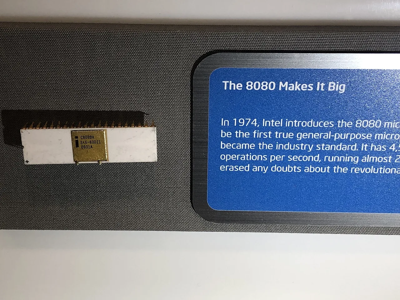
The Intel 8080 was more than an incremental upgrade from the 8008. It was a complete 8-bit parallel CPU designed for general-purpose digital systems, built on Intel’s proprietary n-channel silicon gate MOS process4. Marketed as the “Super 8008”3, it replaced the earlier chip’s complex 24-pin package and limited architecture with a refined design and a full 16-bit address bus (A₀–A₁₅), enabling access to 64 KB of memory, a transformative leap at the time. Data moved over an 8-bit bidirectional tri-state bus (D₀–D₇), while control logic relied on six outputs: SYNC, DBIN, WAIT, WR, HLDA, and INTE, and four inputs: READY, HOLD, INT, and RESET4. Power delivery required three rails: +12V, +5V, and -5V, alongside ground, and it relied on two-phase clock inputs (φ₁ and φ₂), typical of NMOS designs of the era.
Priced at either $24.95 for the C8080 variant3 or $24.50 for the standard INTEL 8080 CPU13, the chip was, in 1976, the sole-source 8080 processor available2. This exclusivity, combined with its architectural clarity, made it a magnet for early adopters. The 8080A revision later improved performance with a 1.5 μsec cycle time, down from the original 8080’s 2.0 μsec8, though the base clock speed remains undocumented in the source material.
Software development was supported by Intel’s own tools, including FORTRAN80, Version 1.0, which functioned as both an assembler and compiler7, and the 8080 Assembly Language Programming Manual (Intel publication #98-004)12. The broader ecosystem leaned heavily on the Intel 8080 Microcomputer Peripherals User's Manual (Order No. 98-364)1415, a document that guided system integrators in connecting memory, I/O, and support chips. The 8080/8085 Assembly Language Programming Manual (Order 98-301) further extended its usability across Intel’s evolving lineup1415.
Its cultural imprint exceeded its technical specs. In 1976, both Intel and the fledgling Microsoft embedded the 8080’s identity into their telephone numbers: Intel’s (408) 987-8080 and Microsoft’s (206) 882-80802. This was no coincidence: it signaled alignment with the 8080 as the de facto standard for mainstream computing at the time. The chip became inextricably linked with the CP/M operating system2, which used its instruction set to create a widely portable microcomputer OS. Though the documentation does not state CP/M as the official OS for the 8080, their fates were intertwined in practice.
The 8080’s influence radiated through compatibility. The Z80, 8085, and even the 8080 itself were listed among compatible processors in Intel’s literature9, with the Z80 ensuring that 8080 codebases could migrate forward. This lineage made the 8080 a pivot point, not because it was the fastest or most elegant, but because it was available, well-documented, and aggressively positioned as a system-building cornerstone.
That said, the surviving documentation is silent on critical details: no release year, no transistor count, no package dimensions, no second-source manufacturers, and no production figures. The gaps are telling. Much of what is commonly attributed to the 8080 (its role in specific machines, its clock speed) rests on external lore, not the primary sources at hand. What remains, however, is clear: the 8080 was a functional, well-supported CPU that Intel positioned as a complete computing engine, not just a logic component. Its design enabled systems that could be programmed, expanded, and standardized, something few earlier processors achieved.
Specifications
| Manufacturer | Intel |
| Product type | 8-bit parallel Central Processor Unit (CPU) |
| Process technology | n-channel silicon gate MOS |
| Data bus | 8-bit bidirectional tri-state (D₀–D₇) |
| Address bus | 16-bit tri-state (A₀–A₁₅) |
| Control outputs | SYNC, DBIN, WAIT, WR, HLDA, INTE |
| Control inputs | READY, HOLD, INT, RESET |
| Clock inputs | φ₁, φ₂ |
| Power inputs | +12V, +5V, -5V, GND |
| Original price | $24.95 (C8080)3 or $24.50 (INTEL 8080 CPU)13 |
| Revision | 8080A with 1.5 μsec cycle time8 |
| Programming | INTEL 8080 language; FORTRAN80 V1.0 assembler/compiler7 |
| Manuals | 8080 Assembly Language Programming Manual #98-00412; Microcomputer Peripherals User's Manual #98-3641415 |
References
- INSITE pgmLibrManVol1 Aug79
- remark-volume9-issue9-1988 (1988)
- 1976 04 BYTE 00-08 Automation (1976)
- 9800132C MDS hwRef Jan79
- Towers International Microprocessor Selector
- MSX Extra 27
- INSITE pgmLibrManVol2 Aug79
- ACS Newsletter 3 7
- AUUGN-V05.5
- 1977 11 BYTE 02-11 Memory Mapped IO (1977)
- 1981 07 BYTE 06-07 Energy Conservation (1981)
- 98-129A MDS800 Operator Manual 1975 (1975)
- 1976 11 BYTE 00-15 More Fun than Crayons (1976)
- 9800616B iSBC 544 Terminal Controller Hardware Reference Manual Dec78
- 9800616A iSBC 544 Terminal Controller Hardware Reference Manual Aug78
- TheMS-DOSEncyclopedia RayDuncan