Motorola 68020
Motorola’s first fully 32-bit microprocessor in the 68000 family, introduced in the mid-1980s, featured an internal instruction cache, coprocessor support, and new instructions that enabled high-performance computing in workstations and early Unix systems.
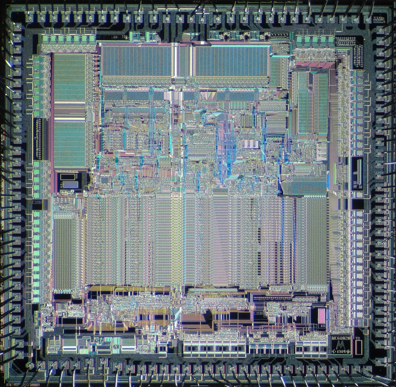
The 68020 marked a definitive break from the hybrid 16/32-bit nature of its predecessors, delivering a true 32-bit implementation of the 68000 architecture with full 32-bit internal and external data paths2. It introduced a 256-byte instruction cache, later clarified as a 64-longword instruction buffer (256 bytes), dedicated solely to instructions, a feature absent in the 68000 and 6801012. This internal cache could be manually disabled via a jumper, a design concession likely intended for debugging or compatibility testing3. The chip employed a three-stage instruction pipeline with overlap, improving throughput over earlier models2.
Architecturally, the 68020 extended the instruction set with operations such as CHK.L, CHK2, RTD, MULS.L, DIVS.L, BFFXXX, and EXTB.L45. These were directly supported by compilers like MPW Pascal, which included a -MC68020 compiler option to generate optimized code; though this rendered applications incompatible with machines lacking the 6802045. Despite these additions, the 68020 maintained upward compatibility with the 68000, allowing legacy code to run without modification7.
The processor supported external coprocessors, most notably the 68881 floating-point unit, which provided full IEEE 754-compliant 80-bit floating-point arithmetic including transcendental functions2. From the programmer’s perspective, the pair appeared as a single integrated processor2. It also supported the 68851 PMMU (Paged Memory Management Unit), enabling demand-paged virtual memory systems1. The 68020 itself operated in both 24-bit and 32-bit processing modes, offering flexibility during the transition from earlier 68000-based systems14.
System-level implementations varied. One documented configuration, the Altos 3068EP, included 2 MB of DRAM expandable to 16 MB15. That system also featured an 8 KB two-way set-associative cache on the processor board, distinct from the internal 256-byte instruction cache15. Another configuration described a 16 KB board-level cache available for both data and instructions1. The Altos 3068EP operated with zero wait states when sourcing from cache15.
Motorola projected shipments of 75,000 units for the year 1985, indicating early commercial momentum7. The chip was adopted in several notable systems, including the Sun-3 series16, HP 9000 Series 200/300 workstations2, the Macintosh LC14, and the Altos 3068EP15. In HP systems, the 68020 was validated using HP-UX, with engineers conducting instruction integrity and virtual memory capability tests, particularly around instruction continuation after interrupts, and reporting bugs directly to Motorola for correction in subsequent mask revisions2. Margin testing on new mask sets included low-voltage and high-temperature stress conditions to improve reliability2.
Software environments included UNIX System V Release 2.215, Sun systems running Release 4.116, and HP-UX2. Some systems shipped with minimal software; the Motorola Bug monitor was the only software included with certain 68020-based platforms8. Migration between systems was constrained: programs could move between 68020 and 68030 boards due to similar floating-point handling, but not to or from 68040-based systems, which introduced incompatible instructions like move166.
Clock speeds reported in system documentation include 16 MHz14, 16.67 MHz12, and 25 MHz12, though discrepancies (e.g., 16.7 MHz15 vs. 16.67 MHz) suggest variations across implementations or rounding differences. The lack of a stated original chip price in surviving documentation is notable. Source 3 references a $895 price, but this pertains to the DSI-020 coprocessor board, not the standalone 680203.
Specifications
| Architecture | 32-bit implementation of the Motorola 68000 architecture |
| Internal instruction cache | 256 bytes (64 longword instructions) |
| Instruction pipeline | Three-stage with instruction overlap |
| Coprocessor support | 68881 FPU, 68851 PMMU |
| Processing modes | 24-bit and 32-bit |
| Reported clock speeds | 16 MHz, 16.67 MHz, 16.7 MHz, 25 MHz |
| Virtual memory support | Demand-paged virtual memory |
| Extended instructions | CHK.L, CHK2, RTD, MULS.L, DIVS.L, BFFXXX, EXTB.L |
| Compiler support | MPW Pascal with -MC68020 option |
| System cache (board-level) | 8 KB or 16 KB, data and instruction |
| Main memory (example system) | 2 MB DRAM, expandable to 16 MB |
| Memory organization | Not specified in sources |
| Shipment volume (1985) | 75,000 units (projected) |
References
- 2537240-0001 68020cpu Dec86
- HP Journal 1986-09 (1986)
- 1986 08 BYTE 11-08 Object-Oriented Languages (1986)
- MPW 3.0 Pascal 1988 (1988)
- MPW Pascal 3.0 Reference 1988 (1988)
- 2549448-0001F TI System V Release 3.3.1 Information Apr92
- 1985 07 BYTE 10-07 Computers and Space (1985)
- The Rainbow Vol. 05 No. 06 - January 1986 (1986)
- Programming The M68000 1983 Addison-Wesley Publishing Company (1983)
- 813-2004-14 CardcageSlotAssignments&BackplaneConfigRevA 29Sep88 (2004)
- PN 072-0228 Apple Service Technical Procedures Macintosh Family Volume Two-Mar 1992 (1992)
- Altos 3068EP brochure
- 800-3805-10 System&NetworkAdministrationRevA 27Mar90